How scientists grow multi-coloured 2D perovskites in a single pot
Researchers developed a one-pot sequential crystallisation method to grow different 2D perovskite semiconductors side by side in a single flat sheet.
Reading level
The full story with proper science words explained.
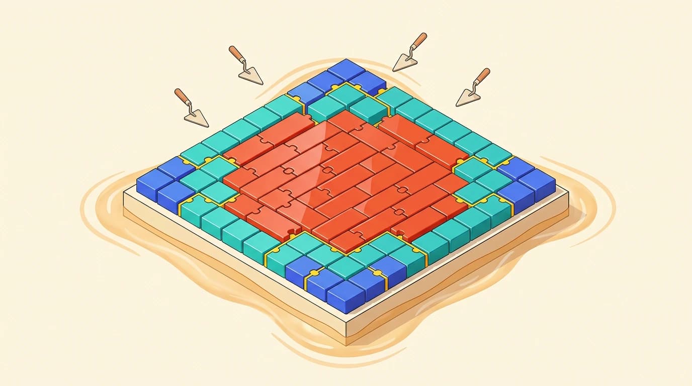
Connecting flat crystals edge to edge
What if you could build complex electronic junctions inside a single flask, just by getting the timing right? Most chips rely on semiconductors, substances that control electric currents. When scientists combine varied semiconductors, they create a heterostructure—a joined piece that steers the flow of charges. Assembling these side by side in ultra-thin sheets of 2D perovskites—crystal semiconductors just atoms thick—is usually very difficult.
Growing side by side
The team solved this using sequential crystallisation. Instead of making separate pieces and gluing them edge to edge, they grew the crystals step by step in one pot. They started growing one 2D perovskite seed in liquid. Next, they timed injections of fresh precursors carrying distinct halides or metal cations. This forced a new crystal zone to sprout directly from the outer rim of the first one, forming a lateral heterostructure in the exact same flat plane.
Think of it like paving a patio with red bricks first, then laying grey bricks outward from the rim. They share the same level floor, even though the blocks differ. Unlike simple stone, crystal lattices only link neatly if their building blocks fit together.
What the lab tests showed
The resulting sheets had high crystal quality with seamless joins between zones. By alternating feeds, the team made sheets with multiple heterojunctions, which are the boundaries where two unlike semiconductors meet. The sheets showed multicolour emission and clear optical coupling, meaning light energy shifted smoothly across the borders between zones. Notably, the study focused on making the sheets and checking their optical traits, rather than testing complete working gadgets.
What we still do not know
Precise control over fluid mixes and injection timing is needed to avoid flawed shapes. The team did not report production yields, working lifetimes, or performance data. We also do not yet know which specific light-based tools, such as lasers or LEDs, can be made using this single-pot process.
Science words
- 2D perovskites
- Ultra-thin, sheet-like crystal semiconductors that confine electric charges to a flat plane.
- heterostructure
- A structure made of different semiconductor materials joined together.
- sequential crystallisation
- A chemical method where distinct crystal regions are grown one after another in a set order.
- lateral heterostructure
- A material where different semiconductors meet edge-to-edge within the exact same flat sheet.
- heterojunction
- The boundary interface where two distinct semiconductors join.
- optical coupling
- The transfer and interaction of light energy across adjacent material zones.
Check it yourself
This story is based on a real research paper in Advanced Materials by Faraji, Schleusener, Khabbaz Abkenar et al. We write with AI help and check it against the paper, but the original is the final word.