How a Miniature Golf Course for Light is Advancing Topological Photonics
Source PublicationNano Letters
Primary AuthorsDüreth, Gagel, Laibacher et al.
Imagine you are designing a miniature golf course for a ball made entirely of pure light. If the bumpers are rough or the channels are too shallow, your light ball simply scatters into the ether. You need perfectly smooth, deep trenches to guide the light exactly where you want it to go, especially around sharp corners.
For years, physicists have struggled to build these microscopic light courses on computer chips. They want to trap and steer light to build faster, more efficient technologies. This forms the basis of topological photonics, a field that aims to control light in incredibly precise ways.
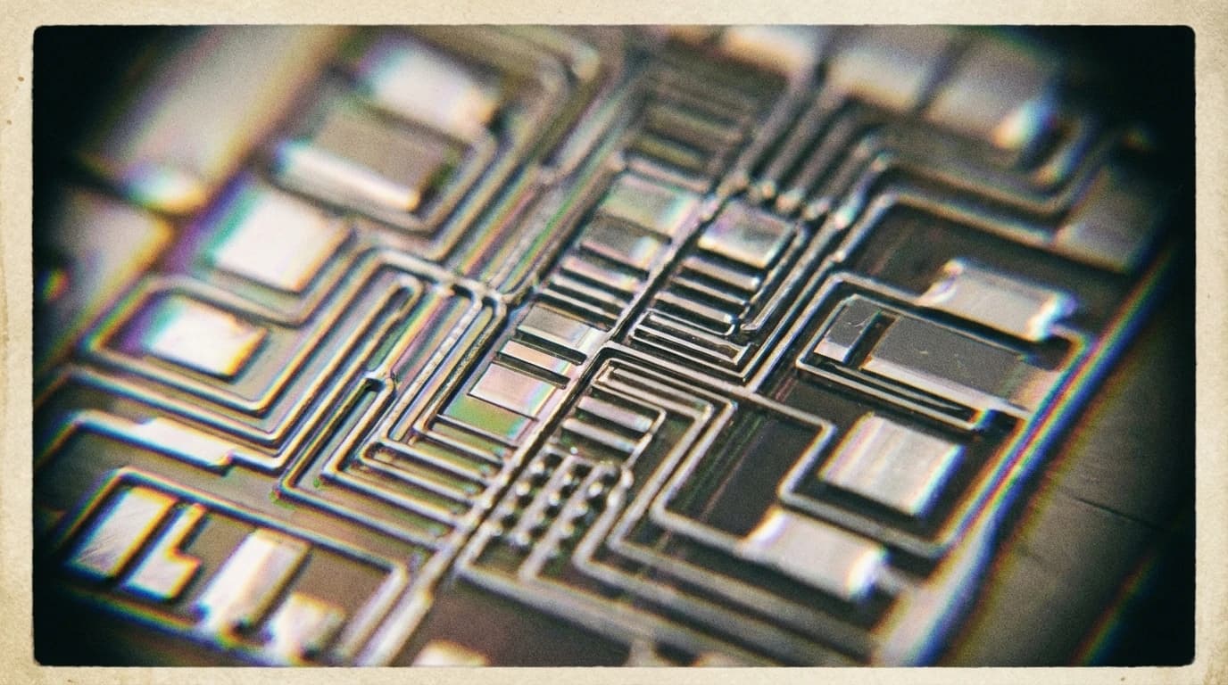
However, standard manufacturing methods have a major flaw. Traditional techniques, like deep ion etching, act a bit like a tiny chainsaw. They carve out the channels but leave rough, damaged edges that cause the light to leak away.
A Smoother Path for Topological Photonics
To fix this, a team of researchers tested two new fabrication methods. Instead of violently carving deep into the semiconductor chip, they gently shaped the surface. They then coated the entire structure with a sputtered dielectric mirror layer.
The team calls these methods "etch-and-oversputter" and "deposit-and-oversputter." This hybrid approach measured significantly better at keeping the light trapped inside the channels. It maintained the high quality of the materials while creating deep, highly controllable pathways.
To prove it worked, the researchers tested their new method on a microscopic basket-weave pattern known as a Kagome lattice. They successfully observed highly specific light emissions—called polariton lasing—right in the corner of this structure.
This measured observation confirms they achieved tight polariton localisation. In other words, they proved they can trap and control light particles in incredibly tight, specific spots without them scattering away.
Building the Next Generation of Light Chips
By proving they can confine light so tightly without losing its quality, the researchers have created new engineering options. This smoother manufacturing technique suggests a clear route to making advanced optical computing a reality.
Specifically, this approach could allow engineers to build:
- More complex, intricate lattices on standard microchips.
- Higher-order insulators that protect light signals from scattering.
- On-chip quantum simulators that use trapped light to perform advanced calculations.
We are not quite at the stage of putting these quantum light chips in your smartphone. However, the study suggests that by giving light a perfect track to run on, the future of optical computing is closer than ever.